The components that make up computer chips are very small. With billions of transistors in a single processor, each made of multiple materials carefully arranged in patterns as thin as a strand of DNA, their manufacturing tools must also operate at a molecular level.
Typically, these tools involve using stencils to pattern or remove materials with high fidelity, layer after layer, to form nanoscale electronic devices. As chips must fit more and more components to keep up with the digital world, these stencils must also become smaller and more precise.
A team of Penn Engineers demonstrated how a new class of polymers could do that. In a new study, the researchers demonstrated how multi block copolymers can produce patterns in thin films that are smaller than three nanometers.
Karen Winey is a professor in the Departments of Materials Science and Engineering and Chemical and Biomolecular Engineering, and Jinseok Park is a graduate student in her lab. They collaborated with Professor Mecking of the University of Konstanz.
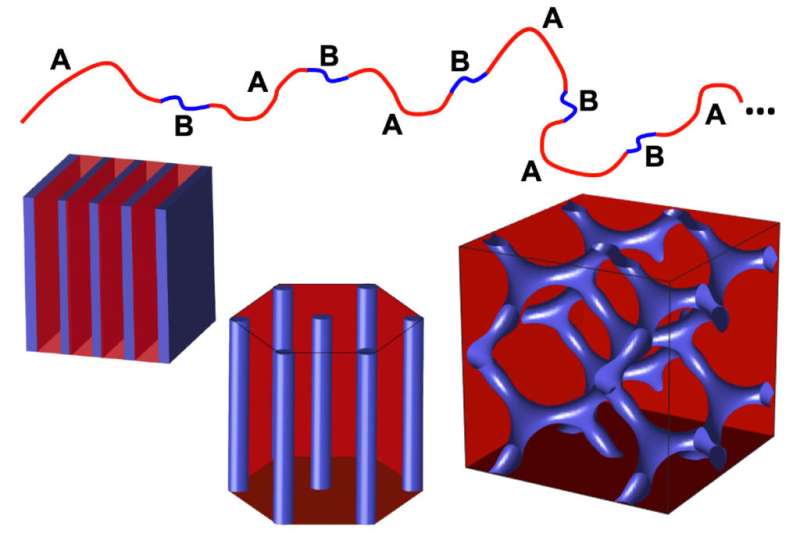
A variety of methods can be used to create the nanoscale patterns in the stencils. Fine lines and small dots can be created by directed self assembly (DSA), a technique where the chemistry is designed so that it automatically produces the desired geometry.
DSA methods use two long blocks of different polymers bonding end to end, which then assemble to produce the necessary patterns.
When photolithography could not go any smaller, DSA with diblock copolymers became important.
Blocks in a diblock copolymer form lines or dots with some variability in their dimensions, decreasing their usefulness as stencils.
Penn and Konstanz researchers came up with a way to control the ratio. Instead of sticking two big blocks of different polymers end to end, they use a technique known as step growth polymerization to alternate between two smaller blocks.
Winey says that multiblock copolymers offer a wider range of chemistries and greater control. The A-blocks and B-blocks are exactly the same length, which will produce greater uniformity in the pattern.
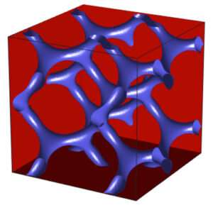
One critical difference this uniformity can make is the ability for thepolymer to more easily assemble itself into a double-gyroid structure within a thin film. The arrangement separates the polar and non polar regions of the polymers, which is useful for controlling transport properties.
Winey says that the continuous non-polar domain provides mechanical strength and that it can promote conductivity of charged or polar species.
The researchers are trying to figure out how to convert these thin film structures into functionalnanopatterning stencils and develop a library of different multiblock chemistries that can form double gyroid structures.
More information: Jinseok Park, Anne Staiger, Stefan Mecking, and Karen I. Winey, Ordered Nanostructures in Thin Films of Precise Ion-Containing Multiblock Copolymers, ACS Central Science (2022). DOI: 10.1021/acscentsci.1c01594 Journal information: ACS Central Science Citation: A new class of materials for nanoscale patterning (2022, March 24) retrieved 24 March 2022 from https://phys.org/news/2022-03-class-materials-nanoscale-patterning.html This document is subject to copyright. Apart from any fair dealing for the purpose of private study or research, no part may be reproduced without the written permission. The content is provided for information purposes only.All Rights Reserved © 2024


