
The building blocks of a quantum computer are similar to the transistors in a classical computer. Superconducting qubits are still measured in millimeters, despite engineers being able to shrink transistors to nanometer scales. A practical quantum computing device could not be smaller than a phone.
MIT researchers have used ultrathin materials to build superconductivity qubits that are at least one-hundredth the size of conventional designs and suffer from less interference between neighboring qubits. The advancement could improve the performance of quantum computers and allow the development of smaller quantum devices.
The researchers have shown that hexagonal boron nitride, a material consisting of only a few monolayers of atoms, can be stacked to form the insulator in the capacitors. This defect-free material makes it possible to use smaller Capacitors that are much smaller than those used in a qubit, which shrinks its footprint without sacrificing performance.
The researchers show that the structure of these smaller capacitors should reduce cross-talk, which occurs when one qubit unintentionally affects surrounding qubits.
For practical use in the future, we will need thousands or millions of qubits in a device. It will be important to miniaturize the size of each individual qubit and at the same time avoid the unwanted cross-talk between these hundreds of thousands of qubits. This is one of the few materials we found that can be used in this kind of construction.
The co-lead author is Megan Yamoah, a former student in the Engineering Quantum Systems group who is currently studying at Oxford University. The senior author is William D. Oliver, a professor of electrical engineering and computer science and of physics. Nature Materials published the research today.
Qubit quandaries.
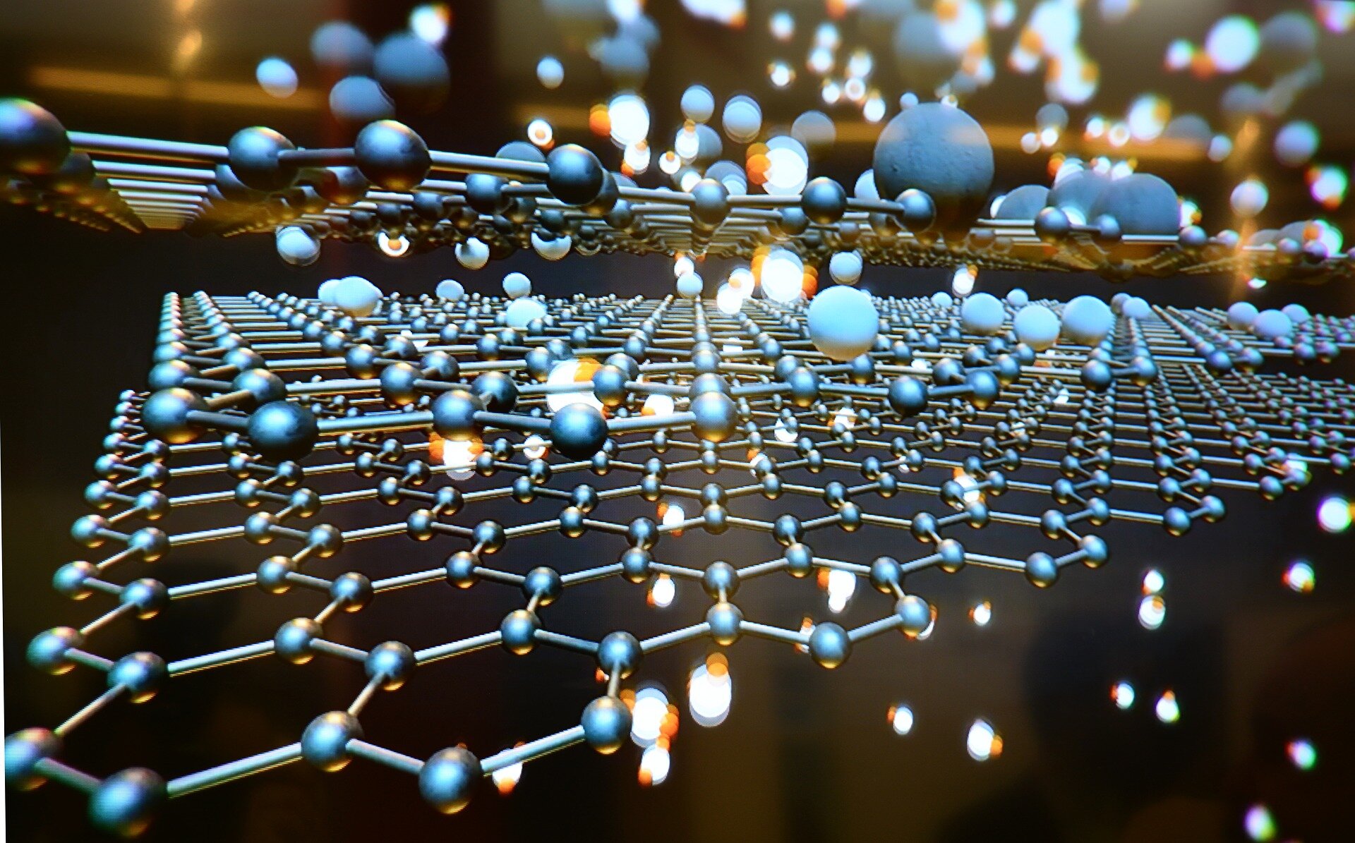
Superconducting qubits, a kind of quantum computing platform that uses superconducting circuits, have inductors and capacitors. The electric field energy is stored in the capacitors. A sandwich of metal plates on either side of a material is called a Capacitor.
Superconducting quantum computers have very high-frequency electric fields similar to cellphones, and operate at super-cold temperatures. The majority of the materials that work in this regime have defects. It is not detrimental to most classical applications when quantum-coherent information passes through the dielectric layer.
Quality factors can be as high as 500 to 1,000 for most common dielectrics used for integrated circuits. Oliver says that this is too lossy for quantum computing applications.
Conventional qubit capacitors are more like open-faced sandwiches, with no top plate and a vacuum sitting above the bottom plate to act as the insulation layer.
The price one pays is that the plates are much bigger because you use a larger layer for the vacuum. When you have two qubits next to each other, and each has its own electric field open to the free space, it can be hard to control just one qubit. One would love to go back to the original idea of aCapacitor, which is just two electric plates with a very clean insulator sandwiched in between.
These researchers did that.
They thought hexagonal boron nitride, which is from a family known as van der Waals materials, would be a good candidate to build aCapacitor. This unique material can be Thinned down to a single layer of atoms that are not defects. Researchers can stack those thin layers.
They ran experiments to find out how clean the material is when interacting with a high-frequency electric field at ultracold temperatures, and found that very little energy is lost when it passes through the material.
Much of the previous work was done using DC transport measurements. In the gigahertz regime, qubits operate. It is great to see that hBN capacitors have quality factors exceeding 100,000 at these frequencies, amongst the highest Qs I have seen for lithographically defined, integrated parallel-plate capacitors.
Capacitor construction.
They used hexagonal boron nitride to build the parallel-plate capacitor. The van der Waals material niobium diselenide was sandwiched between hexagonal boron nitride.
The fabrication process involved preparing one-atom-thick layers of materials under a microscope and then using a sticky polymer to grab each layer and stack it on top of the other. They melted the sticky polymer and washed it away after placing it on the qubit circuit.
The qubit was cooled to 20 millikelvins after they connected theCapacitor to the existing structure.
One of the biggest challenges of the fabrication process is working with niobium diselenide, which oxidizes in seconds if exposed to the air. The whole assembly of this structure has to be done in the glove box, which is a big box filled with a very low level of oxygen. Wang says that they have to do everything inside the box.
The qubit is 100 times smaller than what they made with traditional techniques. The lifetime of the qubit is only a few microseconds shorter with their new design. According to Wang, the electric field between the upper and lower plates is more than 90 percent of the electric field between other qubits. This work is related to research done by a team at Columbia University.
The researchers want to use this method to build many qubits on a chip to verify that their technique reduces cross-talk. They want to improve the performance of the qubit by fine tuning the fabrication process or even building the entire qubit out of 2D materials.
We have cleared a path to show that you can safely use as much hexagonal boron nitride as you want. This opens up a lot of possibilities where you can combine a microwave circuit with a variety of different Heterostructures, and there is a lot more room to explore. Wang says that people can use this material in any way they want without worrying about the loss that is associated with the dielectric.
More information: Joel Wang, Hexagonal boron nitride as a low-loss dielectric for superconducting quantum circuits and qubits, Nature Materials (2022). DOI: 10.1038/s41563-021-01187-w. www.nature.com/articles/s41563-021-01187-w Journal information: Nature Materials Citation: Ultrathin materials may pave the way for personal-sized quantum devices (2022, January 27) retrieved 27 January 2022 from https://phys.org/news/2022-01-ultrathin-materials-pave-personal-sized-quantum.html This document is subject to copyright. Apart from any fair dealing for the purpose of private study or research, no part may be reproduced without the written permission. The content is provided for information purposes only.All Rights Reserved © 2024


