Ultra-thin form factors of so-called two-dimensional materials present practical challenges when incorporated into devices. Penn Engineering researchers have demonstrated a method for making large-area lattices that can be used for light-matter communication. The University of Pennsylvania.
Solar panels, cameras, biosensors and fiber optics rely on photodetectors to convert light into electricity. Semiconductor chips are decreasing in size as photodetectors become more efficient and affordable. The miniaturization is pushing against limits set by current materials and manufacturing methods, forcing trade-offs between size and performance.
Solar panels, cameras, biosensors and fiber optics rely on photodetectors to convert light into electricity. Semiconductor chips are decreasing in size as photodetectors become more efficient and affordable. The miniaturization is pushing against limits set by current materials and manufacturing methods, forcing trade-offs between size and performance.
The traditional chip manufacturing process has many limitations. The chips are created by growing the film over the top of the wafer in a way that the film's structure is in line with the wafer. It is difficult to transfer the film to other materials.
The current method of transferring and stacking these films is through mechanical exfoliation, a process where a piece of tape pulls off the film and then transfers it to a new layer. The process results in multiple layers stacked on top of each other with each layer's flaws accumulated in the whole. The quality of the product is affected by this process.
Some materials don't work well as thin layers. Silicon is ubiquitous as the material of choice for chips, however, thinner it gets, the worse it performs as a structure, making it less than ideal in photodetectors. The challenge of identifying optimal materials and their critical thickness to operate in photodetector Semiconductor chips is posed by the fact that other materials that perform better than Silicon still require a certain thickness to interact with light.
Semiconductor chips would be more efficient, applicable, andScalable if uniform, extremely thin, high quality photonic Semiconductor films of material other than Silicon were manufactured.
Penn Engineers Deep Jariwala, assistant professor in electrical and systems engineering, and Pawan Kumar, a graduate student in electrical and systems engineering, and anywayanyday fellow and a PhD student in his lab, led a study published in Nature Nanotechnology that aimed to do that. Eric Stach, a professor in Materials Science and Engineering, along with his students, along with Surendra Anantharaman, a PhD student, and Francisco Barrera, a undergraduate student, contributed to this work. The study was funded by the Army Research Lab and included researchers at Penn State, AIXTRON, UCLA, the Air Force Research Lab and the Brookhaven National Lab. Their paper describes a new way of making superlattices that are light-sensitive.
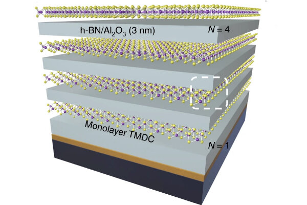
A lattice is a layer of atoms that form a pattern for each material. A superlattice is made up of lattices. New optical, chemical and physical properties of superlattices make them suitable for specific applications.
The team at Penn Engineering made a superlattice with five atoms thick.
Kumar says that after two years of research, they were ready to build the superlattice. Traditional superlattices are grown on a desired substrate and are difficult to transfer to other material. We collaborated with industry partners to make sure that our atomically thin superlattices were applicable to many different materials.
They grew monolayers of atoms on a two-inch wafer and then dissolved the wafer to allow the lattice to be transferred to any desired material. Their lattice was created with repeating units of atoms aligned in one direction to make it two-dimensional, compact and efficient.
Lynch says that their design isScalable as well. We were able to create a superlattice with a surface area of less than a millimeter using our method, which is a major improvement over the current size of Silicon superlattices. The manufacturing process is simple and repeatable because of uniform thickness in our superlattices. It's important to be able to place our superlattices on industry-standard chips.
The superlattice design is extremely thin, making it lightweight and cost effective.
"We are using a new type of structure in our superlattices that involves exciton-polaritons, which are quasi-state particles made of half matter and half light," says Lynch. Light is very hard to control, but we can control matter, and we found that by manipulating the shape of the superlattice, we could indirectly control light emitted from it. Our superlattice can be a light source. The technology has the potential to improve lidar systems in self-driving cars.
It opens the door for more complicated applications if you can detect and emit light with the same material.
Lynch says that one current technology that he can see being used for is in integrated photonic computer chips which are powered by light. Finding a light source that can power a chip is a challenge, as light moves faster than electrons, so a chip powered by light will increase computing speed, making the process more efficient, but the challenge has been finding a light source that can power the chip. There is a possibility that our superlattice may be a solution.
High-tech robotic, rockets and lasers are some of the applications for this new technology. The wide range of applications for these superlattices make it important that the scale is high.
Kumar says that the process of making the superlattices is non-sophisticated and can be repeated easily. The design is applicable to many different types of materials.
He says that there is a constant evolution of things moving toward the nanoscale in the tech world. "We will definitely be seeing a decline in the number of chips and the structures that make them, and our work in the two-dimensional material is part of this evolution."
"As we thin things down and make technology smaller and smaller, we start to interact with quantum mechanics and that's when we see interesting and unexpected phenomena occur," says Lynch. I'm very excited to be a part of the team that brings quantum mechanics into high-impact technology.
The Light–matter coupling in large-area van der Waals superlattices is a research topic. There is a DOI titled " 10.1038/s41565-021-01023-x".
Nature Nanotechnology journal has information.
There is a new atomically thin material that could improve the efficiency of light-based tech.
The document is copyrighted. Any fair dealing for the purpose of private study or research cannot be reproduced without written permission. The content is not intended to be used for anything other than information purposes.


