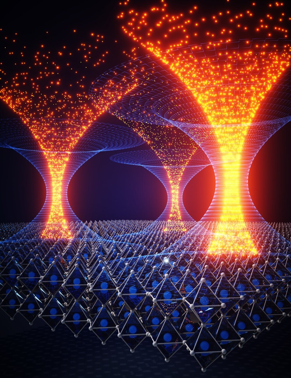
The representation of electrons funneling into the high-quality areas of the material is artistic. Alex T is at the studio.
Researchers from the University of Cambridge have used a suite of microscopy methods to visualize why perovskite materials are so tolerant of defects. Nature Nanotechnology published their findings today.
To achieve efficient energy conversion requires an energy intensive and time consuming production process to create the highly ordered wafer structure, which is the most commonly used material for producing solar panels.
Perovskite materials have emerged as promising alternatives in the last decade.
The lead salts that are used to make them are more abundant and cheaper to produce than the ones that are used to make crystalline Silicon, and they can be prepared in a liquid ink that is printed to make a film of the material. They have great potential for other optoelectronic applications, such as energy efficient light emitting diodes and X-ray detectors.
The performance of the material is surprising. The model for an excellent Semiconductor is a very ordered structure, but the array of different chemical elements combined in Persistries creates a much more messy landscape.
Heterogeneity causes defects in the material that lead to 'traps', which affect the photovoltaic performance of the devices. Despite the presence of defects, the efficiency levels of the materials are still comparable to their Silicon alternatives.
The group has shown that the disordered structure can increase the performance of optoelectronics, and their latest work seeks to explain why.
The group presents a complete picture of the nanoscale chemical, structural and optoelectronic landscape of these materials, that reveals the complex interactions between these competing factors and ultimately shows which comes out on top.
The electronic disorder associated with the defects that reduce performance and the spatial chemical disorder that seems to improve it are two forms of disorder.
The bad disorder from the defects can be mitigated by the chemical disorder, which diverts the charge carriers away from the traps that they might otherwise get caught in.
The researchers used several different techniques to look at the same regions in the film. They could compare the results from all these methods to see what's happening at a small scale in these promising new materials.
"We use multiple microscopes to look at the same area of the sample and try to correlate the properties that we pull out of one with the properties we pull out of another one," says Frohna. These experiments are time consuming and resource intensive, but the rewards you get in terms of the information you can pull out are excellent.
The findings will allow the group and others in the field to further refine how they make solar cells.
For a long time, people have thrown the term defect tolerance around, but this is the first time that anyone has visualized it to understand what it actually means to be defect tolerant in these materials.
We can think about how we can mitigate the effects of the other in the most beneficial way, because we know that these two disorders are playing off each other.
The Royal Academy of Engineering Research Fellow at Cambridge's Department of Chemical Engineering and Biotechnology says that the experimental approach has novelty but also cutting edge by itself.
We have given reasons why these materials are defect tolerant. This methodology allows for new routes to perform better for a targeted application. We can look at other types of perovskites that are good for solar cells, as well as for LEDs or detectors, and understand their working principles.
The set of acquisition tools that we have developed in this work can be extended to study any other optoelectronic material, something that may be of great interest to the broader materials science community.
Sam Stranks, University Assistant Professor in Energy at Cambridge's Department of Chemical Engineering and Biotechnology, says that through these visualization, we now understand the landscape of the semiconductors.
The results show how the field has driven the high performance of mixed composition perovskites. blueprints for design of new semiconductors that may have similar attributes have been revealed.
The optoelectronic response of alloyed perovskite solar cells is dominated by the chemical heterogeneity. www.nature.com/articles/s41565-021-01017-9
Nature Nanotechnology journal has information.
There is a mystery of high performing novel solar cell materials revealed in stunning clarity.
The document is copyrighted. Any fair dealing for the purpose of private study or research cannot be reproduced without written permission. The content is not intended to be used for anything other than information purposes.


