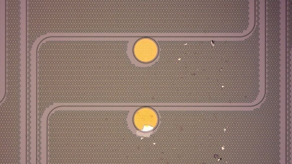
TOS-doped graphene has a high conductivity but absorbs very little infrared light from the resonator. This combination of properties makes it unique and promising for optoelectronic applications. Credit: Ipshita Datta, Lipson Nanophotonics Group, Columbia University
This article is about the silicon revolution. Doping is a method that allows researchers to control the current-conducting abilities of silicon. This involves introducing either negatively charged electrons (or "holes") where electrons were once. This allows electricity flow to be controlled. Silicon can do this by injecting other elements, known as dopants, into its three-dimensional (3D), atomic lattice.
However, Silicon's 3D lattice is too large for next-generation electronics. These include ultra-thin transistors and new devices for optical communications. Flexible bio-sensors can also be implanted or worn in the body. Researchers are now experimenting with graphene, a material that is no thicker than one sheet of atoms. The tried-and-true method of doping 3D silicon with 2D graphene isn't possible because it contains a single layer atoms of carbon that don't conduct current.
Researchers have instead of injecting dopants, they have attempted layering on a "charge transfer layer" that adds or subtracts electrons from graphene. Previous methods used "dirty materials" in charge-transfer layers. This would make graphene less doped and hinder its ability to conduct electricity.
A new Nature Electronics study suggests a better way. A multidisciplinary team of researchers led by James Hone at Columbia University and James Teherani in Korea, has described a method to dope graphene using a charge transfer layer of low-impurity, tungsten oxide (TOS).
The new layer was created by the team by oxidizing one atomic layer from another 2D material, tungsten-selenide. When TOS was layered on top of graphene, they found that it left the graphene riddled with electricity-conducting holes. Those holes could be fine-tuned to better control the materials' electricity-conducting properties by adding a few atomic layers of tungsten selenide in between the TOS and the graphene.
Researchers found graphene's electrical mobility (or how quickly charges can move through it) was greater with the new doping technique than any previous attempts. The mobility was further enhanced by adding tungsten selenide spacers. This made the TOS negligible and the intrinsic properties graphene themselves determine the mobility. This combination of high doping with high mobility makes graphene more electrically conductive than other highly conductive metals such as copper and gold.
Researchers said that doped graphene became transparenter as it improved its ability to conduct electricity. Pauli blocking is a phenomenon in which charges that have been altered by doping prevent the material from absorbing light. The graphene was transparent to more than 99 percent at infrared wavelengths. It is essential to achieve high transparency and conductivity in order to transmit information using light-based photonic devices. Information is lost if too much light gets absorbed. This suggests that TOS-doped graphene has a lower loss than other conductors. It could be a promising method for ultra-efficient photonic devices.
Hone stated, "This is a novel way to tailor graphene's properties on demand." "We are just beginning to explore the potential of this new technique."
One promising direction is to modify graphene's optical and electronic properties by changing its TOS pattern, and to imprint electric circuits directly onto graphene. The team is also working on integrating the doped material in novel photonic devices. This could have potential applications in transparent electronics and telecommunications systems as well as quantum computers.
Continue reading Stretching graphene's electronic properties
More information: Min Sup Choi and co, High carrier mobility graphene doped with a monolayer tungsten oxide oxyselenide. Nature Electronics (2021). Information from Nature Electronics Min Su Choi et. al., High carrier mobility graphene doped with a monolayer tungsten oxide, (2021). DOI: 10.1038/s41928-021-00657-y


