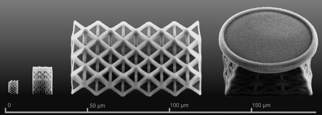
Microscope images show delicate structures created by Rice University materials scientists. They can be sintered into glass or cristobalite. Credit: Nanomaterials Lab, Nanomechanics and Nanodevices Lab
Rice University engineers have made it possible to weave intricate patterns in crystal and glass.
Rice material scientists are developing nanostructures of silica using a sophisticated 3D printer. This allows them to create micro-scale electronic, mechanical, and photonic devices starting from the bottom. These products can be doped, and their crystal structures can be tuned for different applications.
Jun Lou, a professor of material science and nanoengineering at George R. Brown School of Engineering published the study in Nature Materials.
Silicon, the fundamental semiconducting material for microprocessors, is the foundation of electronics. Rice's study challenges the limits of top-down manufacturing and turns the process upside down.
Lou stated that it is very difficult to create complicated, three-dimensional geometries using traditional photolithography techniques. It's not very green because it involves a lot more chemicals and steps. Even with all the effort, certain structures are not possible to create with these methods.
He stated that "in principle, we can print any 3D shape, which could be very useful for making exotic photonic device," "That's what our goal is to demonstrate."
The two-photon-enabled printing process for silica structures at sub-200 nanometer resolution is shown in a cutaway diagram. Credit: Nanomaterials Lab, Nanomechanics Lab and Nanodevices Lab
Two-photon polymerization is used in the lab to produce structures that are several hundred nanometers wide and smaller than the wavelengths of light. The lines are "written" by lasers. They cause the ink to absorb two light photons and initiate free-radical polymerization.
Boyu Zhang, a Rice graduate student and coauthor of this article, said that normal polymerization is involving polymer monomers and photoinitiators. These molecules absorb light and create free radicals.
He said that photoinitiators absorb two photos at once, which takes a lot energy. Polymerization can only be caused by a very small peak in this energy, and it happens in a very limited space. This is why we can go beyond the diffraction limit.
Rice Lab had to create a new ink for the printing process. Zhang and co-lead writer Xiewen, a Rice alumnus created resins containing nanospheres made of silicon dioxide, doped with polyethylenegl to make them soluble.
The structure is then solidified by high-temperature Sintering. This removes any polymer and leaves amorphous glass, or polycrystalline Cristobalite. Lou explained that the material changes from glass to crystal when heated and the higher the temperature the better the crystals are.
The lab also demonstrated the use of rare earth salts to dope the product, making it photoluminescent. This is an important property in optical applications. Next, the lab will refine the process to attain sub-10 nanometer resolution.
The paper's co-authors are Hua Guo (Rice assistant researcher), Guanhui Gao (research scientist Guan Zhang), alumnus Yushun Zhou, and Qiyi Fang, and Christine Nguyen, Rice alumnus; Shuai Yue, University of Houston alumnus, who is now a postdoctoral researcher with the Chinese Academy of Sciences; Jiming Bao, a professor of electric and computer engineering at University of Houston; and Jiming Bao
More information: Xiewen Wen et al., 3D-printed silica at nanoscale resolution, Nature Materials (2021). Information from Nature Materials Xiewen Wen et al., 3D-printed silica at nanoscale resolution. (2021). DOI: 10.1038/s41563-021-01111-2


