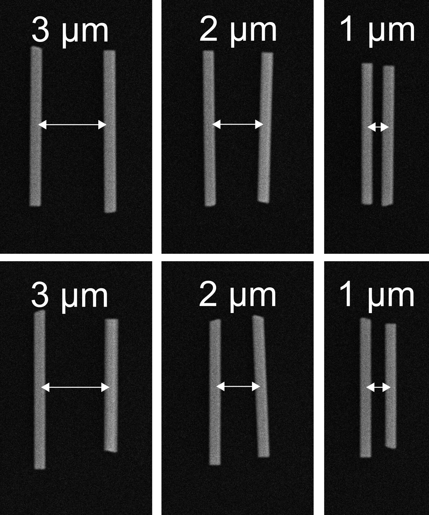
Researchers have developed a method to make multiple nanoscale optical devices very close together on one chip. The transfer printing process was demonstrated by placing nanotubes at a distance of 1 to 3 microns. Credit: Dimitars Jevtics University of Strathclyde
Researchers have created a method to build multiple micron-scale optical components on one chip. This new method could eventually allow for high-volume production of chip-based optical system that will enable advanced imagers and compact optical communications devices.
Dimitars Jevtics, University of Strathclyde, UK says that electronics based on silicon transistors have enabled more powerful and flexible system on a chip. However, optical systems on a chip require the integration of multiple materials and have not seen the same level of development as silicon electronics.
Jevtics and his colleagues present their new transfer printing process in the Optica Publishing group journal Optical Materials Express. They demonstrate how it can place multiple materials on a single chip and that they can integrate them within a footprint as small as the devices. This new method is a better alternative to other methods that only use one material. Future system designers will be able to draw from a wider range of materials.
Jevtics stated that on-chip optical communications will, for instance, require the assembly and integration of optical sources, channels, and detectors onto sub-assemblies which can be integrated with silicon chip. Our transfer printing process could be scaled to incorporate thousands of devices made from different materials onto one wafer. This would allow micron-scale optical devices that can be integrated into future high-density computer chips or lab-on-a chip bio-sensing systems to be used.
Better way to choose and place
It is difficult to put multiple devices on one chip together. Researchers developed a method that uses reversible adhesive to allow a device to be lifted from its growth substrate and placed on a new surface.
Researchers also developed a multi-wavelength, nanolaser system using semiconductor nanowires placed on silicon dioxide. This new method of transfer printing could allow for high-volume production of optical systems based on multiple materials. Credit: Dimitars Jevtics University of Strathclyde
This new method employs a soft-polymer stamp mounted on a robot motion control stage to grab an optical device from its substrate. After the substrate is placed on top of the suspended device, it can be aligned with a microscope to ensure that it is perfectly aligned. After aligning properly, the two surfaces come into contact. This releases the polymer stamp from the device and deposits it onto its target surface. This approach was possible thanks to advances in micro-assembly robotics and nanofabrication techniques.
Jevtics stated that by carefully designing the stamp's geometry to match the device, and controlling the stickiness with the polymer material we can engineer whether the device will be picked-up or released. This process is safe and does not cause any damage when optimized. It can also be automated to scale up for wafer-scale manufacturing.
A densely packed chip
The researchers combined aluminum gallium arsenide optical resonators with diamond and gallium trioxide to demonstrate their new technique. The integration was successful because the optical resonators had good optical transmission.
The printing method was also used to create semiconductor nanowire-lasers by placing nanowires on host surfaces in densely spaced arrangements. The spatial separation of the nanowires was measured using scanning electronic microscopy. This accuracy was within the 100-nanometer region. They were able create a multi-wavelength, nanolaser system by placing semiconductor nanowires onto silicon dioxide.
Jevtics stated that this printing technique isn't limited to optical devices as a manufacturing method. "We hope electronics specialists will also be able to see the potential for how this could be used in future systems."
The researchers plan to continue their research by attempting to reproduce these results using larger numbers of devices in order to prove that it works on larger scales. The researchers also plan to combine their transfer printing method with an automated alignment technique that they have previously developed to allow rapid measurement, selection, and transfer of hundreds more isolated devices for use in imaging and hybrid optics.
Further reading: Patterning silicon at the one nanometer scale
More information: DimitarsJevtics et.al, Spatially dense integra-tion of micron-scale device from multiple materials on a single-chip via transfer-printing. Optical Materials Express (2021). Journal information: Optical Materials Express Dimitars Jevtics et al, Spatially dense integration of micron-scale devices from multiple materials on a single chip via transfer-printing,(2021). DOI: 10.1364/OME.432751


