From the perspective of a traditional x86 computing enthusiastor professionalmainframes are strange, archaic beasts. They are physically large, powerful, and more expensive than traditional data-center gear. In general, they offer less compute per rack at higher costs.
The question is "Why continue using mainframes?" The cynical answers which boil down to "because it's how we always done it" are a bit limiting. Practical answers, however, can be found in reliability and consistency. AnandTech's Ian Cutress explains in a speculation piece about the Telum's new cache that "downtime of these [IBM Z] system is measured in milliseconds each year." If true, that would be at least seven nines.
IBM's announcement of the Telum suggests how different mainframe computing and commodity computing priorities are. The Telum's memory interface is described as "capable to tolerating complete channel failures or DIMM malfunctions" and "designed to transparently recover data with no impact on response time."
If you take a DIMM from a running x86 server, it does not "transparently retrieve data". It simply crashes.
IBM Z-series architecture
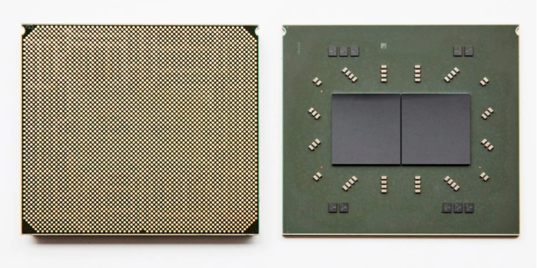
Telum is designed to be something of a one-chip-to-rule-them-all for mainframes, replacing a much more heterogeneous setup in earlier IBM mainframes.
Telum's 14 nm IBM z15 processor is being replaced by five processors, two pairs of 12-core Compute Processors, and one System Controller. Each Compute Processor has 256MiB L3 cache that is shared among its 12 cores. The System Controller, however, hosts a staggering 960MiB L4 cache that is shared between all four Compute Processors.
Advertisement
Five of these z15 processorseach consisting of four Compute Processors and one System Controllerconstitutes a "drawer." Four drawers can be combined in one z15-powered mainframe.
While the idea of multiple processors for a drawer or multiple drawers for a system is still valid, Telum's architecture is significantly different and simplified.
Architecture by Telum
Telum looks a lot simpler than z15. It's an eight core processor built on Samsung 7nm process. Two processors are combined in each package, similar to AMD's chiplet strategy for Ryzen. All of the processors in Telum are identical, so there is no need for a separate System Controller processor.
Four Telum CPU packages are combined to create a four-socket "drawer" and four of those drawers will go into a single mainframe. There are 256 cores total on 32 CPUs. Each core operates at a base clockrate of over 5 GHz, which provides more predictable and consistent latency in real-time transactions than a lower base clockrate with a higher turbo rate.
Caché-filled pockets
The central System Processor was removed from each package. This meant that Telum's cache had to be redesigned. Also, the huge 960MiB L4 cache and the per-die shared, L3 cache were gone. Each core in Telum has its own 32MiB private L2 cache. There is no hardware L3 and L4 cache.
This is where things get really weird. Although each Telum core's 32MiB L2 memory cache is technically private it is actually only almost private. The processor searches for empty space in L2 caches of other cores when a line is removed from one core. If it finds any, the processor tags the L2 cache line that was evicted from core x as an L3 line and stores it in core y’s L2.
Advertisement
Okay, now we have a virtual L3 cache that can be shared with up to 256MiB on each Telum processor. It is composed of 32MiB of each core's L2 cache. The sharing of 256MiB (virtual) L3 on each processor is possible to be shared as "virtualL4" between all processors within a system.
The "virtual L4" of Telum works in a similar way as its "virtual L3". L3 cache lines that were evicted from one processor are now looking for a new home on another processor. If another processor within the Telum system has spare space, the L3 cache line is retagged L4 and moved to the virtual L3 of the other processor. This L3 (which is comprised of eight cores' "private" L2s) replaces the L3 one-way.
Ian Cutress, AnandTech's director of Information Technology, gives more details about Telum's cache mechanism. He finally summarizes them by asking "How is that possible?" With a simple "magic"
Artificial intelligence acceleration
Telum also offers a 6TFLOPS On-Die Inference Accelerator. It is intended to detect fraud in real-time during financial transactions, rather than shortly after.
IBM uses multiple needles to achieve maximum performance and minimum latency. IBM has placed the new inference accelerator on-die. This allows for lower latency interconnects between accelerator cores and CPU cores. However, it is not embedded into cores, as Intel's AVX512 instruction set.
In-core inference acceleration such as Intel's has the problem of limiting AI processing power to any one core. A Xeon core running AVX512 instructions has only the hardware within its core. Larger inference jobs need to be divided among multiple Xeon Cores to get the best performance.
Telum's accelerator runs on-die, but is off-core. This allows one core to run inference workloads using the full power of the entire accelerator.
Listing image by IBM


