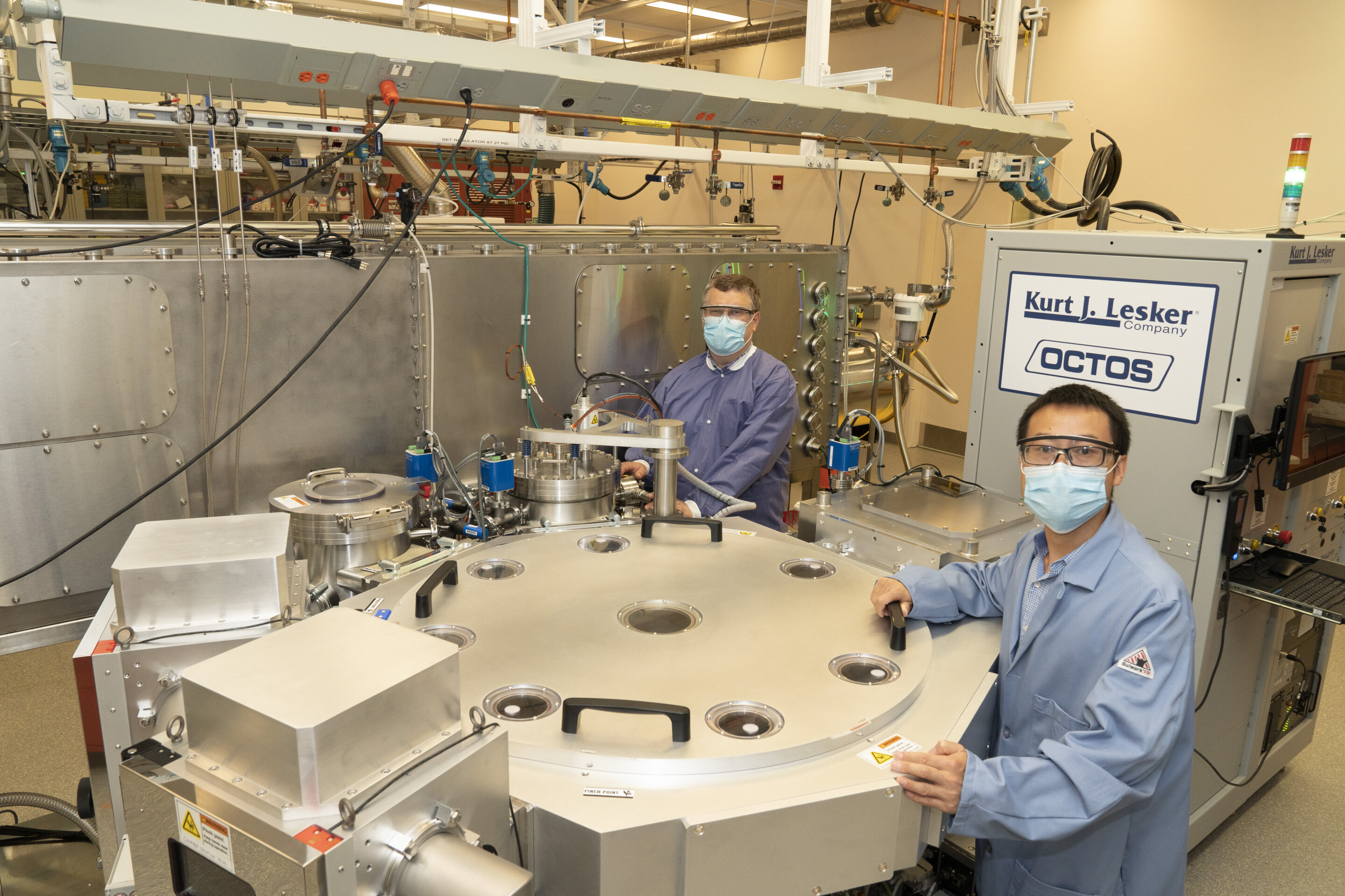
Jurek Sadowski, staff scientist (left), and Zhongwei Dai, postdoc at the Quantum Material Press facility at Brookhaven National Laboratory's Center for Functional Nanomaterials. The central QPress robot is represented by the large circular piece. It has various modules attached to the sides for sample annealing and film deposition, plasma cleaning, sample libraries, and plasma cleaning. The complete QPress system is still in development. It automates the stacking of 2-D materials to create layers with exotic properties for quantum-related applications. Credit: Brookhaven National Laboratory
Two different bilayer graphene configurations were studied by scientists. They are the two-dimensional (2D) and atom-thin forms of carbon. Scientists have detected optical and electronic interlayer resonances. These resonant states are where electrons bounce back-and-forth between the two atomic planes at the 2D interface at the exact same frequency. These states were characterized by the authors. They found that twisting graphene layers 30 degrees relative the other shifts the resonance energy to a lower level. This result was published in Physical Review Letters. It showed that the distance between layers in the twisted configuration was significantly greater than the stack one. Interlayer interactions change with distance, which can have an impact on how electrons move within the bilayer system. Understanding the electron motion can help design future quantum technologies that are more powerful and secure for communication.
"Today's computer chip is based on our knowledge of electrons moving in semiconductors, specifically silicon," stated Zhongwei Dai (first and co-corresponding author), a postdoc at the Center for Functional Nanomaterials at the U.S. Department of Energy's Brookhaven National Laboratory. The physical properties of silicon are reaching limits in terms of the size of transistors that can be made and the number of chips that can accommodate them. We may be able unlock another way to use electrons for quantum information science if we understand how electrons move on a very small scale, just a few nanometers, in 2D materials.
A few nanometers (or billionths of meters) is the equivalent of an electron's wavelength. The material's optical and electronic properties can change when electrons are contained in a space that is the same size as their wavelength. These quantum confinement effects occur due to quantum mechanical wave-like motion and not classical mechanical motion in which electrons move through materials and are scattered by random imperfections.
The team used a simple model material, graphene, to investigate quantum confinement effects. They also applied two probes, electrons (particles light) and photons (particles). They used a special substrate to transfer graphene onto in order to probe both optical and electronic resonances. Jurek Sadowski, a co-author and a scientist in the CFN Interface Science and Catalysis Group, had previously created this substrate for Quantum Material Press (QPress). CFN Materials Synthesis and Characterization Facility is currently developing the QPress, an automated tool for the synthesis and processing of layered 2D material. Scientists exfoliate 2D material "flakes", from 3D parent crystals (e.g. graphene from graphite), on a silicon dioxide substrate a few hundred nanometers thick. This substrate is insulating so electron-based interrogation techniques won't work. Sadowski, Chang-Yong Nam, a CFN scientist, and Ashwanth Subramanian, a Stony Brook University graduate student, deposited a conductive layer made of titanium oxide that was only three nanometers thick onto the silicon dioxide substrate.
Sadowski explained that this layer is transparent enough to allow optical characterization and determinations of thickness of exfoliated flakes and stacked monolayers, and it's conductive enough to enable electron microscopy and synchrotron-based techniques.
The University of Pennsylvania's Charlie Johnson Group, where Qicheng Zhang and Zhaoli Gao, former postdocs at the Chinese University of Hong Kong, grew graphene on metal foils and transferred it onto a titanium oxide/silicon dioxide substrate. All three domains of graphene (single, stacked and twisted) can be observed when graphene has been grown this way.
(a) Schematics for the experimental setup of electron and photon scattering. (b) Anatomic model of the pattern created by the twisted bilayergraphene (30-tBLG), crystal structure. Low-energy electron microscope image showing a typical sample area with 30-tBLG, single-layer graphene and stacked bilayer graphene. (d) Low-energy electron diffraction patterns on a 30-tBLG region. Credit: Brookhaven National Laboratory
Dai and Sadowski then designed and conducted experiments where they shot electrons into the materials with a low energy electron microscope (LEEM), and detected the reflected electrons. They also used a laser-based optical microscope equipped with a spectrometer to fire photons into the material. The spectrum of light that was scattered back was also analyzed. The QPress cataloger includes a confocal Raman microscope, as well as image-analysis software that can be used to pinpoint the location of areas of interest.
Dai said, "The QPress Raman microscope allowed us to quickly identify our target sample area and accelerate our research."
The results showed that the spacing between layers of the twisted graphene configuration was six percent greater than the non-twisted. The unique electronic behavior of the twisted configuration was confirmed by calculations made at the University of New Hampshire by theorists.
Sadowski stated that devices made from rotated graphene could have unusual and surprising properties due to the increased interlayer spacing where electrons can move.
The team will then fabricate devices using the twisted graphene. CFN staff scientist Samuel Tenney, and CFN postdocs Calley Eads & Nikhil Tiwale conducted initial experiments to determine how different materials can be added to the layered structure to alter its electronic and optical properties.
Dai stated, "In our initial research, the simplest 2D materials system we could synthesize and control to understand electrons' behavior" "We intend to continue these types fundamental studies, hopefully shedding some light on how to manipulate material for quantum computing and communication."
Further exploration Specially oriented, twisted bilayer graphene hosts topological electron states
Further information: Zhongwei Dai et. al., Quantum-Well Bound States In Graphene Heterostructure Interfaces, Physical Review Letters (2021). Information for the Journal: Physical Review Letters Zhongwei DAI et al. Quantum-Well Bound States In Graphene Heterostructure Interfaces, (2021). DOI: 10.1103/PhysRevLett.127.086805


