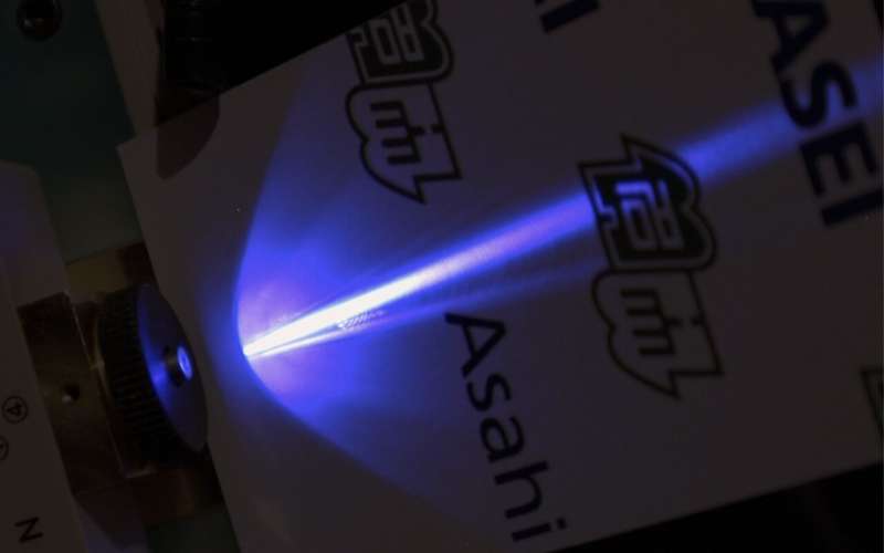
The world's first room temperature continuous-wave lasing has been conducted by a research group led by Hiroshi Amano at Nagoya University's Institute of Materials and Systems for Sustainability.
The results published in Applied physics Letters represent a step towards widespread use of a technology with the potential for a wide range of applications.
After decades of research and development, successful commercialization of laser diodes has been achieved for a number of applications. There are examples of this technology in optical communications devices.
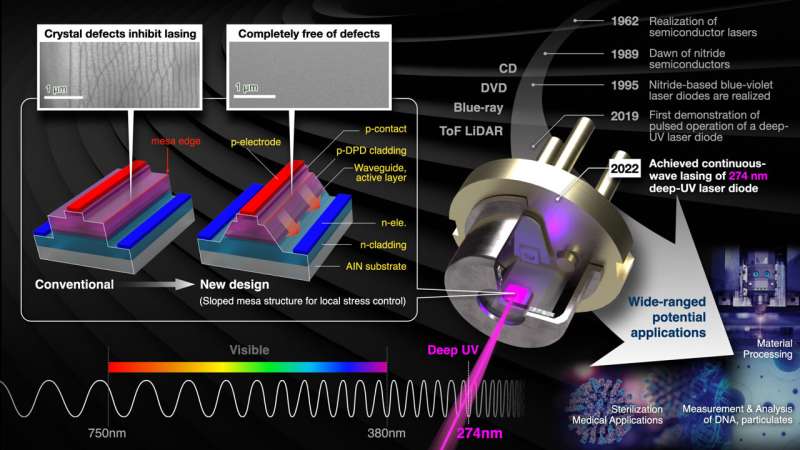
Despite the efforts of research groups around the world, no one was able to develop deep ultravioletLDs. The emergence of technology to fabricate aluminum nitride (AlN) substrates, an ideal material for growing aluminum gallium nitride (AlGaN) film for UV light-emitting devices, was a key breakthrough.
Professor Amano's research group collaborated with the company that provided 2-inch AlN substrates to develop a deep-ultra violet LD. It was difficult to get enough current into the device.
The research group was able to solve the problem using a technique called polarization-Induced Dopamine. This is the first time that they have produced a short-wavelength UV-CLD. The input power was too high for continuous- wave lasing because it would cause the diode to heat up and stop lasing.
The structure of the device has been changed to reduce the drive power needed for the laser to work. Crystal defects at the laser stripe cause earlier devices to require high levels of operating power. The strong crystal strain created these defects.
By tailoring the side walls of the laser stripe they were able to suppress the defects and reduce the operating power.
The development of the new UV laser technology was made possible by the Center for Integrated Research of Future Electronics. Under C-TEFs, researchers from partners such as Asahi Kasei share access to state-of-the-art facilities on the Nagoya University campus, giving them with the people and tools needed to build high quality devices.
A representative of the research team was in his second year at the time. He told an interviewer that he wanted to do something new. Professor Amano told me that the time was right for ultraviolet, despite the fact that everyone assumed it was impossible.
Semiconductor lasers can be used in all wavelength ranges. In the future, UV-CLDs could be used for healthcare, virus detection, particulate measurement, gas analysis, and high-definition laser processing.
It could be a ground-breaking application to sterilizing technology. Lasers can be used to destroy large areas in a short time. Surgeons and nurses could benefit from this technology.
Two papers about the results have been published.
There is more information about local stress control to suppress dislocation generation for pseudomorphically grown AlGaN UV-C lasers. It's called 10.1063/5.0124512.
The Key temperature- dependent characteristics of AlGaN-based UV-C laser diodes and demonstration of room-temperature continuous-wave lasing was presented by Hiroshi Amano and his team. The DOI is 10.1063/ 5.0124480.
Journal information: Applied Physics Letters
All Rights Reserved © 2024


