We've found a number of materials that are atomically thin. Some of these sheets are made from a single element while others are formed from chemicals. There are many different materials that have different properties. A number of others are also conductors of electricity. Depending on how you arrange the layers of a multi-sheet stack, you can tune their properties further.
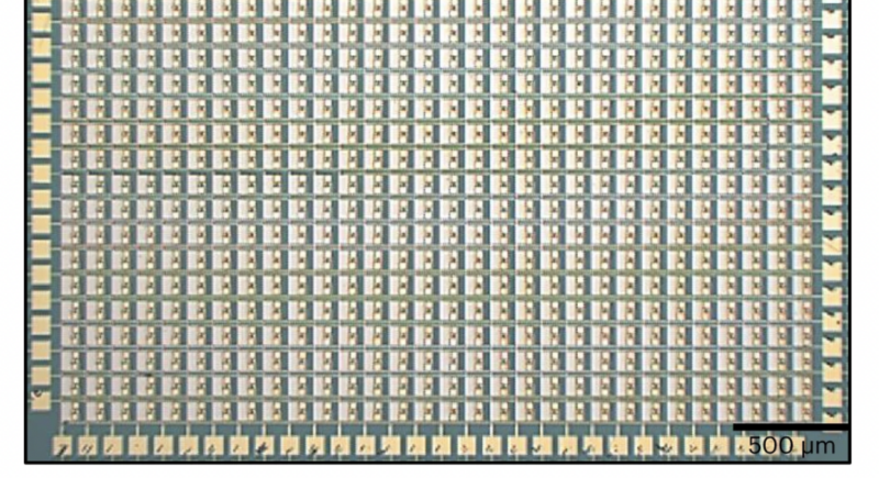
It shouldn't be a surprise to anyone that researchers have figured out how to make electronics out of these materials. The hardware demonstrations are not integrated into a useful device. A team of researchers have shown that it is possible to build a 900-pixel sensor using atomically thin material.
The majority of image sensors are made using the usual CMP processes. It is possible to replace the Silicon with a different type of Semiconductor. Molybdenum disulfide is an atomically thin material that has been used in many experimental devices.
The researchers started by growing a single-layer sheet of Molybdenum disulfide on a sapphire. It was lowered onto a previously madeSilicon dioxide surface that already had some wiring etched into it. There was more wiring deposited.
This process resulted in a 30 by 30 grid of devices, each consisting of a source and drain electrode with a sheet of Molybdenum disulfide connecting them. Stray charges can affect the ability to transmit current between the source and drain electrodes. The difference in resistance gives a measure of how much light the device was exposed to, which can be used to reconstruct images.
AdvertisementMost devices apply a strong voltage between the source and drain electrodes to clear the charges that build up after exposure to light.
It's a bit of a mixed bag when you compare it to a standard Silicon sensor. The researchers estimate that it takes less than a PicoJoule to operate the devices. The process of setting the device is easy.
The researchers found a way to make it light. The signal-to-noise sensitivity of the image sensor can be adjusted. Normally, this requires a lot of external circuitry on the hardware, with an increase in manufacturing complexity and power use. This device has some advantages.
It doesn't offer fast. A full, high-contrast exposure takes seconds per color, even though the initial response to light can be as little as 100 seconds. A blue exposure takes over two seconds, and a red exposure takes over 10 seconds. Don't expect this to be used to take quick videos on your cell phone.
This doesn't mean it's useless, but it limits what it can do. Environmental sensors and the like are examples of applications where power is more important than time. The researchers built a large, complicated device that relied on atomically thin material.
Nature materials About DOIs can be found here.
All Rights Reserved © 2024


