Scientists at the U.S. Department of Energy's Brookhaven National Laboratory have developed a new way to guide the self-assembly of a wide range of novel nanoscale structures. Miniature medieval castles and Roman aqueducts can be seen under the nanometer-scale structures that look like Legos. Scientists are looking at how novel shapes might affect a material's function.
A novel approach to control self-assembly is described in a paper just published. The analysis shows that different shapes have different electrical properties. The work can help guide the design of custom surface coating with tailored optical, electronic, and mechanical properties.
Kevin Yager said that the work opens the door to a wide range of possible applications for scientists from academia and industry. Scientists interested in studying optical coating, or electrodes for batteries, or solar cell designs could tell us what properties they need, and we can choose the right structure from our library of exotic shaped materials to meet their needs.
It's automatic assembly.
The exotic materials were made using two areas of expertise. The self-assembly of block copolymers is the first thing that comes to mind. It is possible to see functional shapes in three dimensions using a scanning electron microscope if you use the second method.
Yager said that self-assembly is a great way to make structures. The molecule spontaneously organizes into the desired structure when you design it.
Blocks of long chainlike molecule called block copolymers are deposited onto a substrates. The two ends of the block copolymers want to separate from each other. The two ends of the copolymer move as far apart as possible while still being connected. A new structure is created by the reorganization of chains.
Scientists use metal or other substance to make a replica of one of the domains and then burn the original material. A piece of metal or oxide with dimensions that are just billionths of a meter could be useful for a variety of electronics.
It is a powerful andScalable technique. You can cover a lot of areas with these materials. The disadvantage is that the process only forms simple shapes.
Different strategies have been tried by scientists. More complex branching polymers have been tried by some. Microfabrication methods have been used to create small posts or channels that guide where the materials can go. Making more complex materials and the tools and templates that guide them can be both labor- and cost-intensive.
Yager said that they are trying to show that there is an alternative where you can still use simple, cheap starting materials.
Stacking andquenching are done.
Blocks of thin films are deposited in layers.
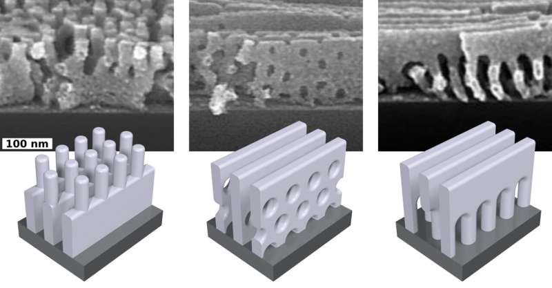
Yager said that they put the two materials on top of each other. More than a dozen exotic structures that haven't been seen before were created by varying the order and thickness of the layers.
Two materials do not want to be grouped together. They want to mix as they get older. New structures are forming because of the mixing.
The layers will eventually form a stable structure if they are allowed to progress. Yager said that by cooling the material rapidly, you can pull out Transient structures and get some other interesting shapes.
Some structures, like the "parapets" and "aqueducts," have features that are derived from the order and reconfiguration of the stacked copolymers.
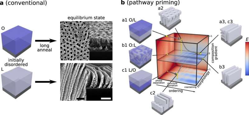
A set of design principles that explain and predict what structure is going to form under a certain set of conditions was created by the scientists. They used simulations to understand how the molecule behaves.
The simulations allow us to see where the individual chains are moving.
Applications that are promising.
The scientists are thinking about how they might be useful. One with parapet-like pillars on top could possibly be a sensor because of its large surface area and electronic connection, Yager suggested.
The first tests focused on electrical conductance. The team replaced one of the newly shaped domains with zinc oxide by using infiltration synthesis. They found huge differences in the electrical Conductivity of the zinc oxide nanostructures.
The same starting molecule is being converted into zinc oxide. The only difference between them is how they're connected to each other at the atomic level. That changes the electrical properties of the final material. It's very important in a sensor for a battery.
The shapes are being explored by the scientists.
Yager said that the next frontier would be multi-functionality. If we want to maximize one property and minimize another, how can we choose a structure that maximizes both?
We have a lot of control with this approach. Using this newly developed method, we can control what the structure is and what material it is made of. We want to work with CFN users on where this approach can lead.
There is more information about Sebastian T. Russell and his colleagues in Nature Communications.
Journal information: Nature Communications
Citation: Self-assembled nanoscale architectures could feature improved electronic, optical, and mechanical properties (2022, November 18) retrieved 18 November 2022 from https://phys.org/news/2022-11-self-assembled-nanoscale-architectures-feature-electronic.html This document is subject to copyright. Apart from any fair dealing for the purpose of private study or research, no part may be reproduced without the written permission. The content is provided for information purposes only.All Rights Reserved © 2024


