A team of scientists from the Department of Energy's Ames National Laboratory have developed a new tool that allows them to gain insight into a possible alternative material for solar cells. Jigang Wang is a senior scientist at Ames Lab and he led the team that developed the microscope. The team used their microscope to look at a material that could be used to make solar cells.
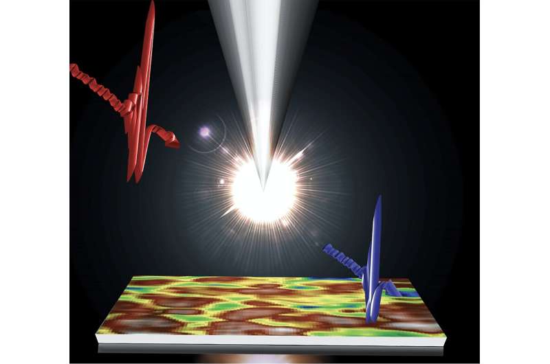
The scanning probe microscope has two features that make it unique. The terahertz range of frequencies is used to collect data. The range is below the visible light spectrum and between the microwaves and the IR. The microscope's capabilities are enhanced by the light shining through a metallic tip.
If you have a light wave, you can't see things smaller than the wavelength of the light. The wavelength of the light is about a millimeter. "Here we used a metallic tip with an apex that is sharper than the wavelength we were using, and this acts as our antenna to see things smaller than the wavelength we were using."
The team used the new microscope to investigate a material called MAPbI 3 that is an alternative to Silicon in solar cells. When exposed to visible light, perovskites transport an electric charge. The main problem with using MAPbI 3 in solar cells is that it degrades quickly when exposed to elements like heat and humidity.
The team expected MAPbI 3 to behave like an insulator when they exposed it. They expected a consistent low-level of light-scatter throughout the material since the data collected on a sample is a reading. Light scattering along the boundary between the grains was different.
Kim explained that a high level of light scattering is what metals have. Light scattering along the grain boundaries in MAPbI 3 sheds light on the degradation problem.
Over the course of a week, the team collected data on the material and it showed the degradation process through changes in the levels of light scatterings. Useful information can be found here.
The study shows a powerful tool to visualize, understand and potentially mitigate grain boundary degradation, defect traps, and materials degradation. It is possible that better understanding of these issues will allow the development of highly efficient perovskite-based photovoltaic devices.
The samples were given to the University of Toledo. Richard H. J. Kim and his co-workers wrote a paper about this research.
There is more information about Richard H. J. Kim's research. The book is titled "acsphotonics.2c00861."
Journal information: ACS Photonics
All Rights Reserved © 2024


