UC Santa Barbara researchers have visualized the photocarrier transport properties of single crystals in a study that confirms their promise as the next-Generation Semiconductor Material.
Bolin Liao is an assistant professor of mechanical engineering in the College of Engineering. He and his team were able to make movies of the generation and transport processes of a photoexcited charge in this relatively little-studied III-V Semiconductor material. The material's potential as the next great Semiconductor was found in the process.
Their research was done in collaboration with a group at the University of Houston who specialize in making high-quality single crystals of Boron Arsenide.
The person is ringing the bell.
Boron arsenide is being seen as a potential replacement for Silicon in the computer world. It is easy to conduct current with an improved charge mobility over Silicon. It also conducts heat in a similar way to Silicon.
The material has 10 times the thermal conductivity of Silicon. As electronic components become smaller and more densely packed, pooled heat threatens the device's performance.
"As your cellphones become more powerful, you want to be able to reduce the heat, otherwise you have inefficiency and safety issues," he said. A lot of microelectronic devices have thermal management challenges.
The high thermal conductivity of this material can lead to interesting transport properties of photocarriers, which are the charges excited by light, for example, in a solar cell. If this is true, it means that the material can be used for light detection and photovoltaics. Due to the small size of available high-quality samples, it has been difficult to measure the photo carrier transport.
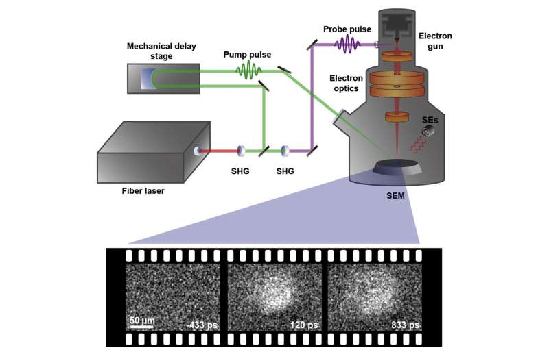
The University of Houston team has the ability to grow crystal, while the UC Santa Barbara team has the ability to image the brain. The UCSB team combined the capabilities of the scanning electron microscope and ultrafast lasers to build a high resolution camera.
Liao said that electron microscopes can resolve single atoms with their sub-nanometer spatial resolution but are typically very slow.
The ultrafast laser acts as a fast shutter for extremely high time resolution with our technique. A millionth of a second is how long it is. We can make films of these processes. At UCSB, the method was further developed and improved from start to finish, and now is the only operational SUEM setup at an American university.
The lead author of the Matter paper explained that the sample was excited by a single pulse of the laser. It's a loud noise that fades over time, like ringing a bell. A second laser pulse is focused onto a photocathode to create a short electron pulse to image the sample. They use the electron pulse to take a picture of the ring. He said that you can get a movie of how the electrons and holes get excited by taking a lot of scans.
Their sample was exciting and they watched the electrons return to their original state.
The hot electrons excited by light in this material can persist for a long time. The hot carriers were seen to persist for more than 200 picoseconds, which is related to the same feature that is responsible for the material's high thermal Conductivity. The ability to host hot electrons for long periods of time has important implications.
When you light the electrons in a solar cell, they have different amounts of energy. The high-energy electrons have a shorter lifetime than the low-energy electrons. When it comes to harvesting the energy from a solar cell, only the low-energy electrons are being collected; the high-energy ones tend to lose their energy quickly as heat. If this material was used as a solar cell, it would be possible to harvest more energy from it.
It has the potential to become the electronics world's next state-of-the-art material if it beats three relevant areas. It faces significant hurdles before it can compete with Silicon, which can be made relatively cheaply and with high quality. Liao doesn't think there's a lot of a problem.
He said that people started developingSilicon around the 1930s and '40s. There will be more effort put into finding ways to grow and use this material once people realize it. UCSB has strong expertise in the field of Semiconductor Development.
More information: Usama Choudhry et al, Persistent hot carrier diffusion in boron arsenide single crystals imaged by ultrafast electron microscopy, Matter (2022). DOI: 10.1016/j.matt.2022.09.029 Journal information: MatterAll Rights Reserved © 2024


