There is still a lot of room at the bottom. The engineers at Rice University are showing how to do it.
A new study describes the discovery of piezoelectricity, the phenomenon by which mechanical energy turns into electrical energy.
The Rice materials scientists, along with their colleagues at the George R. Brown School of Engineering, the University of Southern California, the University of Houston, the Wright-Patterson Air Force Base Research Laboratory and Pennsylvania State University, have their work published.
The discovery could aid in the development of ever-smallernanoelectromechanical systems, devices that could be used to power tiny actuators and implantable biosensors.
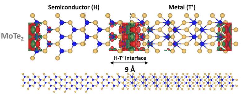
A metallic domain surrounding semiconducting islands creates a mechanical response in the material's crystal lattice when subjected to an applied voltage.
The challenge of making materials with a precise number of layers has been a difficult one, according to the co-lead author of the paper.
Puthirath said that the question was how to make a structure that is piezoelectric at multiple thickness levels. It was possible to make a one-dimensional, metal-semiconductor junction in a 2D Heterostructure.
The group pioneered the idea of atomically sharp boundaries in atomically thin layers. It's possible to engineer materials in 2D to create unique device architectures.
When tellurium gas is introduced, the junction is less than 10 nanometers thick and forms in a chemical Vapor deposition furnace. The sea of metallic phases is created by this process.
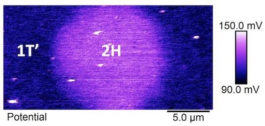
A mechanical response can be generated by applying voltage to the junction. The strength of piezoelectricity is measured.
The phase boundary that is essentially independent of the thickness is created by the difference between the lattice structures. It makes it easier to prepare 2D crystals for applications.
There is more freedom for engineering materials properties with a Heterostructure interface. The asymmetrical nature of the atom may have an influence on the electrical and optical phenomena which are often dominated by the interface.
More information: Anand B. Puthirath et al, Piezoelectricity across Two‐dimensional Phase Boundaries, Advanced Materials (2022). DOI: 10.1002/adma.202206425 Journal information: Advanced MaterialsAll Rights Reserved © 2024


