Tampere University is a university.
A group of researchers at Tampere University have come up with a way to control a light beam with another beam through a plasmonic meta surface. Low intensity of light is required for the linear switch method to work.
The on/off conversion function can be achieved with all-optical switch due to control light. A laser beam can be used to modify a light beam.
The enhancement of index of refraction is a quantum optical phenomenon and is the basis of the switch method developed by the researchers.
The first experimental demonstration of this effect on the optical system is what we have done. The research helps the scientific community to achieve loss-compensated plasmonic devices without using any gain media or processes.
Ultrafast speed is enabled with optical switch.
To avoid the strong dissipation of signal during propagation, high-speed switch and low-loss medium are used. To realize on-chip ultrafast all-optical switch networks, all-optical switch must have ultrafast switch time, ultralow threshold control power, and high switch efficiency.
In all digital electronic devices, signal values of 0 and 1 are fundamental. The electronic elements have become smaller and quicker over the years. The ordinary calculations done with our computers on the order of seconds could not be done with older room-sized computers.
Conventional electronics rely on controlling the flow of electrons on the time scale of a microsecond to a tenth of a second.
Replacing electrons with plasmons can raise the switch speed to an ultra fast time scale. The surface of metals have plasmons on them. She states that this allows optical switch with our device.
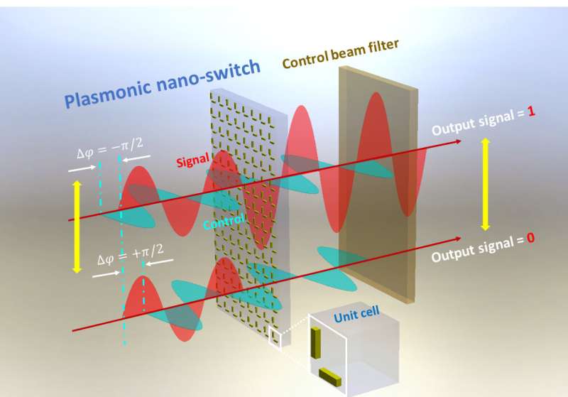
The plasmonic switch has an L-shaped combination of metallicnanorods. The first author of the article published in Nature Communications is a PhD student.
The direction in which the beam is moving is called polarization. Depending on the phase difference between the two beams, the control beam can amplify or diminish the signal. When each beam reaches its maximum intensity, the phase difference is how long it takes. The signal amplification is caused by the transfer of some optical energy from the control beam to the signal through a constructive superposition.
The performance of plasmonic devices can be improved.
When the beams have opposite phase differences, destructive superposition is used to achieve the attenuation of the signal. It has been found that low intensity of light is needed for sustainable use ofnanophotonic devices. The development and realization of nanoscale plasmonic systems can be accelerated by using this simple linear switch method.
Further studies of plasmonic structures and possibly the use of our method in plasmonic circuits are expected. The L-shaped meta surface could be further studied to reveal ultra high-speed switches and to investigate the control of plasmonic particles.
Even more interesting applications and functions can be found in controlling the nanostructures' response to light.
It is possible to enhance the performance of plasmonic devices by creating broadband transparency for a signal beam without any gain medium. Cagalayan says it can open up a number of ways to design smart elements.
More information: Rakesh Dhama et al, All-optical switching based on plasmon-induced Enhancement of Index of Refraction, Nature Communications (2022). DOI: 10.1038/s41467-022-30750-5 Journal information: Nature Communications Provided by Tampere UniversityAll Rights Reserved © 2024


